The Lorenz system, originally discovered by American mathematician and meteorologist, Edward Norton Lorenz, is a system that exhibits continuous-time chaos and is described by three
coupled, ordinary differential equations. The Lorenz system is related to the
Rössler attractor, but is more
complex, having two quadratic nonlinearities rather than just one, and generates a chaotic attractor having two lobes rather than just one. The equations are:
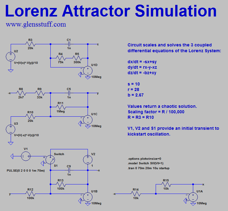
dx/dt = -sx+sy
dy/dt = rx-y-xz
dz/dt = -bz+xy
The behaviour of the system is chaotic for certain value ranges of the three coefficients, s, r and b. The values originally studied by Edward Lorenz were
s=10, r=28 and b=2.67 (8/3). An excellent and much more thorough introduction to the Lorenz system, with references, is available at the Wikipedia page
here.
While the Lorenz attractor is readily simulated with iterative, discrete-type digital computation techniques on a modern desktop P.C., using software packages
such as MATLAB, or even in SPICE with a little more difficulty, it is also readily simulated with simple electronics hardware conforming to a much older concept;
that of continuous analog computation. A complete electrical analog of the Lorenz attractor, as described by the three differential equations above, can be implemented
with an interconnection of just three distinct, basic and common circuit building blocks; namely the summing amplifier, the integrator and the analog multiplier.
Here is my version of a circuit that does just that:
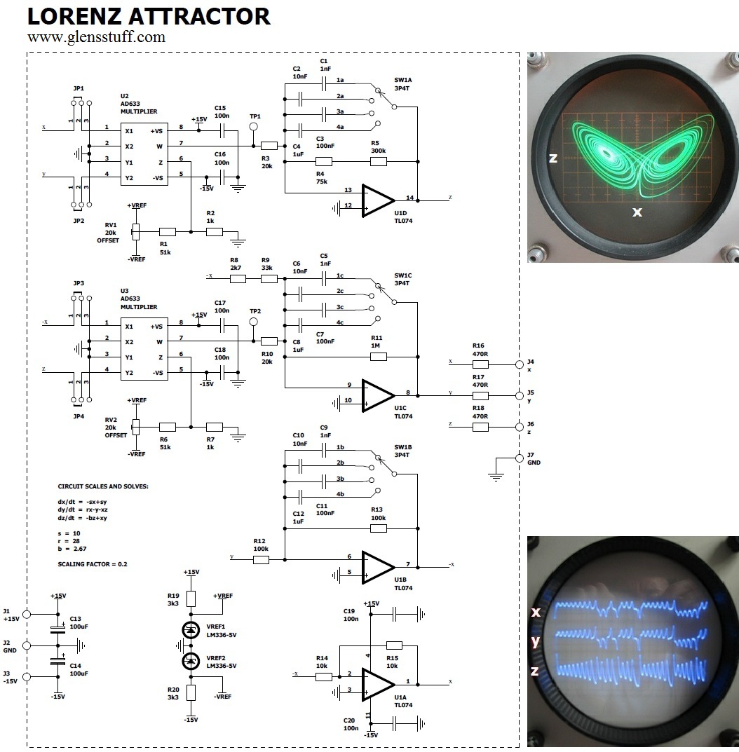
In order to keep the computed and continuously-time variable
x,
y and
z state solutions within the linear operating range of the operational amplifiers
and the two analog multiplier chips running on +/-15V supply rails, a scaling (down) factor of 5:1 was used. Using standard value resistors, the
s,
r and
b
coefficient values were set as close as practical to the values originally studied by Edward. Coefficient
b scales to 1Meg / (R4 + R5). Coefficient
r scales to 1Meg / (R8 + R9)
and coefficient
s scales to 1Meg / R, where R = R12 = R13. The global scaling factor of 5:1 is determined by 0.1Meg / R, where R = R3 = R10. The global scaling factor is
referenced to 0.1Meg rather than 1Meg due to the transfer function of the analogue multiplier integrated circuits, which divide the product of their X and Y input signals by 10.
The phase space of the Lorenz attractor is mapped in the minimal three dimensions required for continuous-time chaos by the three computed states, x, y and z.
The famous "owl face" diagram of the Lorenz attractor is produced by neglecting the y state and plotting the z and x states in two dimensions. This is shown in the
oscilloscope picture incorporated into the schematic diagram above. The x state is plotted on the horizontal axis and the z state on the vertical. However better and
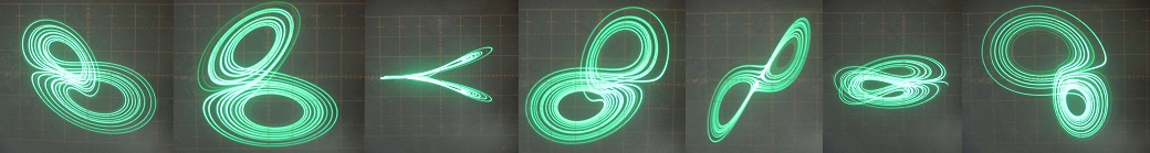
more instructive views can be had by using transformation techniques working with all three states to generate three-dimensional projections on a two-dimensional display.
The series of oscilloscope CRT photos pictured immediately below show three-dimensional projections of the Lorenz attractor at various angles of 2-axis rotation. These displays were
generated by my three-dimensional projective unit, with the Lorenz attractor circuit described here being the x-y-z signal
source.
The operating frequency of the circuit is made variable over a 1000:1 range by the inclusion of switch SW1 and the various integration capacitors, in four decade steps, from approximately
1.5 Hz to approximately 1.5 kHz. Provision has been made to trim the output offset voltages of the two multiplier integrated circuits, U2 and U3. This was found to be necessary as the
accuracy of the solution is sensitive to multiplier offsets to a significant degree. Excessive offset error voltages from the multipliers also proved to make sustained oscillations
unreliable, particularly at higher operating frequencies. The accuracy of the solution appears to be most sensitive to an output offset voltage error from multiplier U3, while sustained
oscillation appears to be more critical to the offset error trim of U2. Offsets are trimmed by placing jumpers J1 through J4 into the 2-3 positions to ground the multiplier X and Y inputs,
then adjusting trimmer potentiometers RV1 and RV2 for 0 mV at test points TP1 and TP2 respectively. Inputs to the multipliers are connected for normal operation by placing all jumpers into the 1-2 position.
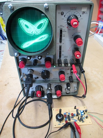
I produced a small PCB for the entire circuit as depicted schematically above; the Gerber files of which can be downloaded via the links at the top of this page, along with the LTspice
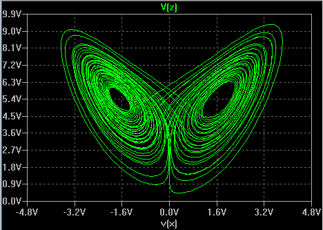
simulation files. The operation of the circuit is simulated in SPICE with a simple transient analysis:
Well, that's it. In conclusion; a rather simple and unusual function generator that makes for a good, demonstrative introduction to analog computation and chaos theory - and a fun
weekend project as well.